A semiconductor facility does not fail or succeed on square footage alone. It rises or falls on infrastructure discipline – the hidden systems that protect yield, stabilize process performance, and keep expansion possible without disrupting production. That is the real answer to what are semiconductor cleanroom infrastructure needs: not just a clean box, but a tightly engineered environment where air, power, water, vibration control, chemical handling, and operational flow work as one system.
For investors and manufacturers, this matters early. The cost of retrofitting a generic industrial building into a semiconductor-capable environment can be far higher than securing a site designed around clean manufacturing from the start. The difference shows up in construction timelines, qualification risk, utility redundancy, ESG performance, and the long-term ability to scale from pilot production to full-volume output.
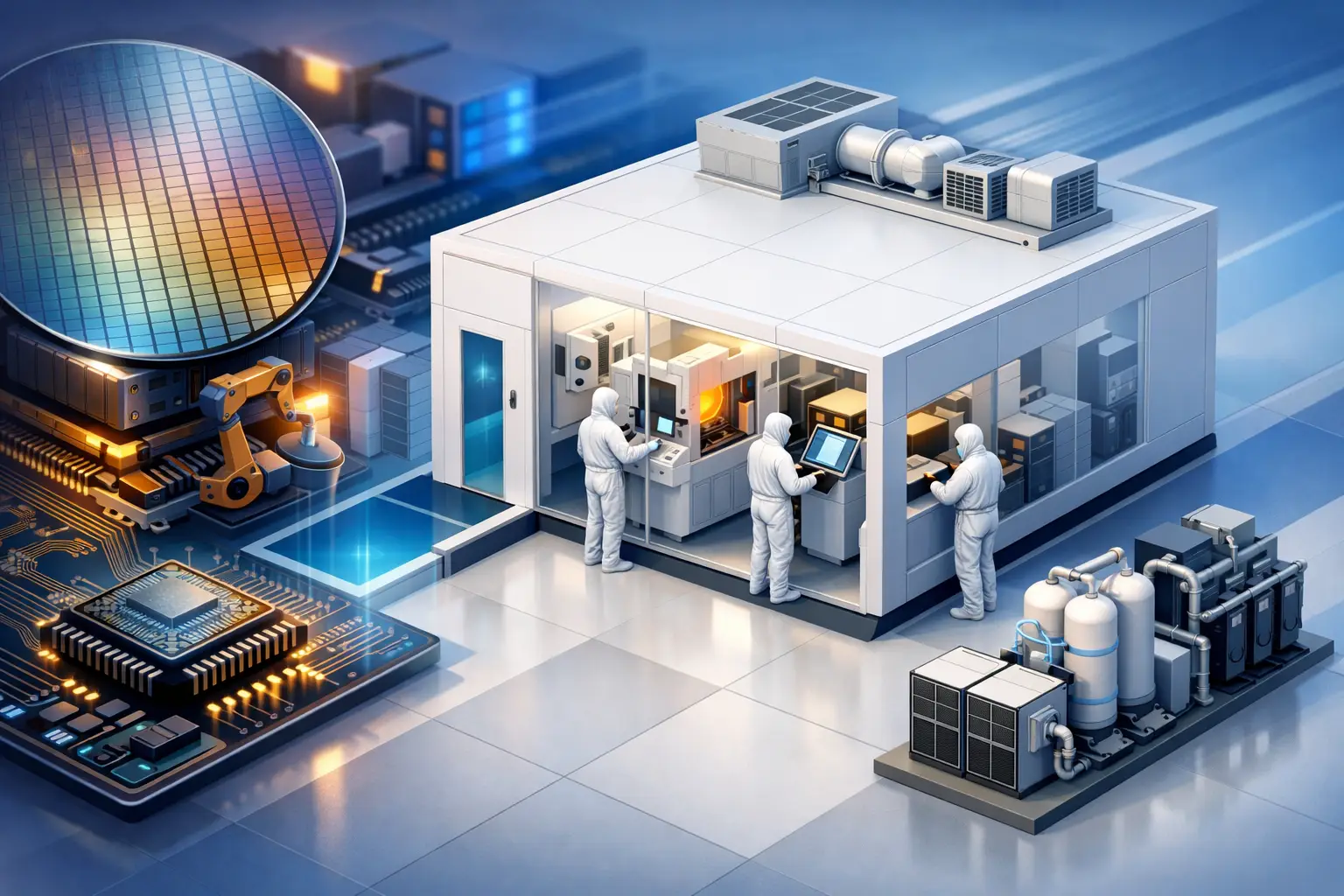
What are semiconductor cleanroom infrastructure needs at a practical level?
At a practical level, semiconductor cleanroom infrastructure needs begin with environmental control, but they do not end there. A wafer fab, backend packaging facility, MEMS line, or compound semiconductor operation may each require different cleanliness classes, process tools, and utility loads. Even so, the core infrastructure stack is broadly consistent: stable structure, controlled airflow, advanced filtration, precise temperature and humidity management, ultra-reliable power, specialty gases, high-purity water, safe waste treatment, and logistics flow that prevents contamination.
That last point is often underestimated. A cleanroom is not only a room. It is a connected operating system that includes gowning areas, material entry, maintenance access, sub-fab space, mechanical floors, chemical storage, monitoring platforms, and emergency response design. If one of those layers is weak, cleanroom performance becomes harder and more expensive to maintain.
The building shell must support process precision
Semiconductor manufacturing starts with the physical building. Floor flatness, structural vibration, ceiling heights, column spacing, and load-bearing capacity all influence tool installation and process stability. Precision equipment cannot compensate for a building that transmits vibration from nearby traffic, HVAC equipment, or adjacent manufacturing lines.
This is why site planning matters as much as interior fit-out. Facilities need the right setback strategy, vehicle routing, and utility zoning to protect the production core from external disturbance. In multi-tenant industrial environments, the semiconductor cluster should be positioned with clear operational separation from heavy mechanical uses that generate dust, heat, or constant vibration.
Expansion capability also belongs in the shell strategy. Semiconductor operators rarely want a site that works only for day one. They want room for future tool sets, utility growth, support buildings, and process changes. That makes modular infrastructure and phased development far more valuable than a one-time build that leaves no margin for scale.
Air quality is the visible requirement, but airflow design is the harder challenge
When people think cleanroom, they think particle control. That is correct, but incomplete. Semiconductor cleanrooms require carefully engineered airflow patterns that remove contaminants consistently across process areas. High-efficiency filtration, pressure differentials, air change rates, and return air design all need to match the process and the cleanroom classification.
The trade-off is energy intensity. The tighter the environmental controls, the greater the HVAC load and the operating cost. That means the right question is not simply how clean the room must be, but where extreme cleanliness is actually required and where supporting spaces can operate at different specifications. Smart zoning protects both yield and cost efficiency.
Temperature and humidity stability are equally important. Semiconductor tools and materials can be sensitive to even small environmental swings. A facility that meets cleanliness targets but drifts on thermal consistency can still create process instability. For manufacturers, this is a reminder that mechanical systems should be designed for performance under real operating conditions, not only for ideal commissioning scenarios.
Power infrastructure must be engineered for continuity, not basic supply
Power quality is a strategic issue in semiconductor operations. Short interruptions, voltage fluctuations, or harmonics can interrupt process tools, compromise batches, and create expensive downtime. Cleanroom-ready infrastructure therefore requires more than grid access. It needs redundancy, backup systems, conditioned power, and distribution architecture aligned with critical loads.
The exact configuration depends on process intensity and risk tolerance. Some facilities need layered backup strategies with generators, UPS support for key systems, and segregated feeds for essential process equipment. Others may prioritize resilience for environmental controls, life safety systems, and data platforms first. What matters is that the electrical design reflects the actual cost of disruption.
For investors evaluating a site, this is one of the clearest signs of seriousness. Industrial land with nominal power availability is not the same as semiconductor-capable infrastructure. Capacity, reliability, future upgrade pathways, and response planning all need to be visible in the development model.
Water, gases, and chemical systems define operational readiness
Semiconductor production depends on utility purity. Ultra-pure water systems, specialty gas distribution, bulk chemical storage, abatement systems, and waste segregation infrastructure are not optional add-ons. They are core components of process integrity and compliance.
Ultra-pure water, in particular, demands careful planning because the infrastructure reaches far beyond pipework. The facility needs treatment systems, recirculation strategy, quality monitoring, and wastewater handling designed around process demand. A weak water strategy can become a production bottleneck or a major ESG liability.
The same is true for gases and chemicals. Safe delivery, containment, leak detection, ventilation, fire protection, and emergency isolation systems must be built into the facility from the beginning. Retrofitting these systems later is not only expensive but can also constrain layout efficiency and regulatory approval.
Sub-fab and support space are often the difference between workable and world-class
A semiconductor cleanroom is supported by an extensive technical backbone below and around the production floor. Sub-fab space houses piping, exhaust, vacuum systems, abatement, cable trays, and maintenance access. Without adequate support space, routine servicing becomes disruptive, and future tool changes become slower and more costly.
This is where many generic conversions fall short. They may offer enough area for the cleanroom itself but not enough technical volume to operate the facility efficiently over time. For leadership teams planning regional expansion, the lesson is simple: usable infrastructure is not measured only by leasable square feet. It is measured by how effectively the building supports uptime, safety, and change management.
Digital controls and monitoring are now baseline infrastructure
Semiconductor facilities require continuous visibility across environmental conditions, utilities, alarms, and energy performance. Building management systems, cleanroom monitoring, fault detection, and data integration are no longer premium features. They are baseline operating requirements for risk control and productivity.
This also has investment implications. Facilities with strong digital infrastructure are easier to validate, easier to optimize, and better positioned for ESG reporting. As advanced manufacturing platforms mature, industrial developers are being judged not only on physical delivery but on how well their assets support measurable operational intelligence.
ESG and compliance are now part of what are semiconductor cleanroom infrastructure needs
A decade ago, some operators treated sustainability as a secondary layer. That position is no longer viable. Energy demand, water intensity, waste management, emissions control, and worker safety now sit close to the center of semiconductor site strategy.
That does not mean every project follows the same path. A high-volume fab and a specialist packaging facility will not have identical utility profiles or compliance burdens. Still, both need infrastructure that can support efficient resource use, transparent reporting, and future regulatory tightening. Developers that plan for recovery systems, efficient HVAC, water recycling, and safer materials management create a stronger long-term value proposition for tenants and investors alike.
This is one reason ecosystem planning is gaining importance. A semiconductor facility performs better when it sits inside an industrial environment designed for advanced manufacturing, workforce support, logistics access, and infrastructure scale. Rana Group’s wider model of integrated industrial development reflects that shift – from isolated buildings to platforms where manufacturing, talent, and support systems can grow together.
Location strategy matters because infrastructure does not exist in isolation
The best cleanroom design can still underperform if the surrounding location creates recurring friction. Logistics access, customs efficiency, workforce availability, utility resilience, permitting clarity, and supplier proximity all shape operating reality. Semiconductor companies entering new markets are not simply buying a facility. They are choosing an infrastructure ecosystem.
This is especially relevant in growth corridors where companies need cost efficiency without compromising technical standards. A location that combines industrial land availability, scalable utilities, port access, and investor-friendly operating conditions can materially improve both project feasibility and speed to market.
For executives asking what are semiconductor cleanroom infrastructure needs, the strongest answer is broader than filtration and finishes. You need a facility engineered for precision, a utility platform built for continuity, and a location strategy capable of supporting the next phase of industrial growth. The future will favor manufacturers that choose infrastructure not as a fixed asset, but as a strategic advantage.
